
TUTORIAL Recuperar deco en "Booting" via JTAG
- Iniciador del tema danilp
- Fecha de inicio
Estás usando un navegador obsoleto. Puede no mostrarse este u otros sitios web correctamente.
Debes actualizarlo o usar un navegador alternativo.
Debes actualizarlo o usar un navegador alternativo.

empiezo a Ubuntu como el primer correo (danilp) todo está bien hacer:
openocd-0.4.0.tar.bz2 tar xjvf
no lo encuentra
de lo contrario (video evolutions) que inicie Windows comand mensaje no puede encontrar openocd \ 0.4.0 \ bin. no hay ninguna carpeta bin que he descargado desde el enlace anterior
¿Existe una solución?
I start ubuntu as the first mail (danilp) all OK to do:
openocd-0.4.0.tar.bz2 tar xjvf
can not find it
otherwise (evolution video) I start Windows comand prompt can not find openocd \ 0.4.0 \ bin. there is no bin folder that I downloaded from above link
is there a solution?
<script src='http://img89.imageshack.us/shareable/?i=screenshotdgl.png&p=tl' type='text/javascript'></script><noscript> </noscript>
pareces a mi dir openocd
look like my openocd dir
<script src='http://img42.imageshack.us/shareable/?i=openocd040.jpg&p=tl' type='text/javascript'></script><noscript> </noscript>
openocd-0.4.0.tar.bz2 tar xjvf
no lo encuentra
de lo contrario (video evolutions) que inicie Windows comand mensaje no puede encontrar openocd \ 0.4.0 \ bin. no hay ninguna carpeta bin que he descargado desde el enlace anterior
¿Existe una solución?
I start ubuntu as the first mail (danilp) all OK to do:
openocd-0.4.0.tar.bz2 tar xjvf
can not find it
otherwise (evolution video) I start Windows comand prompt can not find openocd \ 0.4.0 \ bin. there is no bin folder that I downloaded from above link
is there a solution?
<script src='http://img89.imageshack.us/shareable/?i=screenshotdgl.png&p=tl' type='text/javascript'></script><noscript>
 </noscript>
pareces a mi dir openocd
look like my openocd dir
<script src='http://img42.imageshack.us/shareable/?i=openocd040.jpg&p=tl' type='text/javascript'></script><noscript>
 </noscript>
That seems to be a cable for Elite : I did the same....
pins
db-elite jtag
2-11
3-9
4-7
5-5
13-3
20-2
it's not same !?!
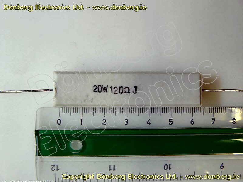
A ver si te ha dicho que de qué "wataje" (que viene de "watt", watio-potencia) las queríasesta mañana he ido a comprar todos los componentes y a la hora de comr las 8 resisitencias de 120 ohmios me dice el voltaje con que las quiero, ya que hay de varios voltajes , me gustaria que me dijerais cual tiene que ser y por lo que estoy leyendo ese puede ser uno de los problemas, muchas gracias y salu2
Dile que las quieres de 1/4 W (de un cuarto de watio), que son las redonditas con colorines

lo mismo el vendedor se ha pensado que eran para un electrodoméstico y te las quería dar de las grandotas
Whaoo ! The list of pins to connect on cable is different : Where did you find this one ?
I've nothing on Jtag pin 11 , for now... Missing in others schemes ?
About your problem : You badly read the doc :
You've to download openocd archive :
wget http://.....
And AFTER :
tar xvf
I've nothing on Jtag pin 11 , for now... Missing in others schemes ?
About your problem : You badly read the doc :
You've to download openocd archive :
wget http://.....
And AFTER :
tar xvf
pins
db-elite jtag
2-11
3-9
4-7
5-5
13-3
20-2
it's not same !?!
With this cabling, the cable does'nt work : It's like no cable was connected
But I'm practically sure the solution is there : On all others receivers, the Jtag requires 6 wires connected to parallel port
Probably the initial document was wrong, but this one too
Who can give us the good wiring ?
Below is the Parallel port DB25 pinout :
Pinouts
Pinouts for parallel port connectors are:
Pin No (DB25) Pin No (36 pin) Signal name Direction Register - bit Inverted
1 1 Strobe In/Out Control-0 Yes
2 2 Data0 Out Data-0 No
3 3 Data1 Out Data-1 No
4 4 Data2 Out Data-2 No
5 5 Data3 Out Data-3 No
6 6 Data4 Out Data-4 No
7 7 Data5 Out Data-5 No
8 8 Data6 Out Data-6 No
9 9 Data7 Out Data-7 No
10 10 Ack In Status-6 No
11 11 Busy In Status-7 Yes
12 12 Paper-Out In Status-5 No
13 13 Select In Status-4 No
14 14 Linefeed In/Out Control-1 Yes
15 32 Error In Status-3 No
16 31 Reset In/Out Control-2 No
17 36 Select-Printer In/Out Control-3 Yes
18-25 19-30,33,17,16 Ground - - -
I took over the archives openocd ubuntu terminal (wget c * ttp: / / download.berlios.de/openocd-0.4.0tar.bz2) and manually from the link but do not see him again?
Duma, where dovnload tar xjvf ?
if anyone else has the same problem with openocd?
pe.tardo,
I have 1 /2 watt resistors
Me hice cargo de los archivos openocd ubuntu terminal (wget c * ttp: / / download.berlios.de/openocd-0.4.0tar.bz2) y de forma manual desde el enlace pero no lo volvería a ver?
Duma, donde dovnload tar xjvf?
si alguien tiene el mismo problema con openocd?
pe.tardo,
Tengo resistencias de 1 / 2 vatio
With this cabling, the cable does'nt work : It's like no cable was connected
But I'm practically sure the solution is there : On all others receivers, the Jtag requires 6 wires connected to parallel port
Probably the initial document was wrong, but this one too
Who can give us the good wiring ?
Below is the Parallel port DB25 pinout :
Pinouts
Pinouts for parallel port connectors are:
Pin No (DB25) Pin No (36 pin) Signal name Direction Register - bit Inverted
1 1 Strobe In/Out Control-0 Yes
2 2 Data0 Out Data-0 No
3 3 Data1 Out Data-1 No
4 4 Data2 Out Data-2 No
5 5 Data3 Out Data-3 No
6 6 Data4 Out Data-4 No
7 7 Data5 Out Data-5 No
8 8 Data6 Out Data-6 No
9 9 Data7 Out Data-7 No
10 10 Ack In Status-6 No
11 11 Busy In Status-7 Yes
12 12 Paper-Out In Status-5 No
13 13 Select In Status-4 No
14 14 Linefeed In/Out Control-1 Yes
15 32 Error In Status-3 No
16 31 Reset In/Out Control-2 No
17 36 Select-Printer In/Out Control-3 Yes
18-25 19-30,33,17,16 Ground - - -
you try like this:
http://www.rdi-board.com/showthread.php?t=37325&highlight=jkeys+by
I made a mistake in the top post.soory
I have a problem with the opening of this forum, very slow to open
Tengo un problema con la apertura de este foro, muy lento para abrir
This forum has nothing to see with Azbox : The target JTAG is totally different (20 pins)
@Terzic :
I think you don't apply the documentation correctly
The wget command is to retrieve the archive on net
LATER, you'll use tar to uncompress it....
It's 2 different steps
@Terzic :
I think you don't apply the documentation correctly
The wget command is to retrieve the archive on net
LATER, you'll use tar to uncompress it....
It's 2 different steps
I find the schema below, about Mips STB Jtag

Considering that, and if we consider the circuit 74HC244 is already on the board, the cabling should be :
DB25 Dir. JTAG
2 (D0) => 11 (RST_N)
3 (D1) => 7 (TMS)
4 (D2) => 9 (TCK)
5 (D3) => 3 (TDI)
6 (D4) => 1 (TRST_N)
11 (Busy) <= 5 (TDO)
20-25 (ground) 2 (ground)
May be TDO is not needed ?
But it's a lot different than the cabling proposed by document !
I'm becoming crazy.....
- 30 Oct 2009
- 43
- 3
- 0
Must respect I/O line definition in IEEE 1149-1 standard ...
to ALL ... For good results ... It's possible to confront with FC_Candido guide's (see: RP1-RP2 on Premium/+ ... or ... RP5-RP6 on Elite m-board) for correct Jtag lines daisy-chained conditions (pull-up +3.3 vdc for TDI-TD0-TMS-NTRST, or adaptive impedence conditions --- see TCK and TD0) and for install additional protective 100 Ohms series resistors (to limit the max current from the Jtag I/O lines)!
Here more info ... h**p://www.interfacebus.com/Design_Connector_JTAG_Bus.html ... extract:
P.S. With not-buffered Jtag-interface the wired lines must to be short ... and don't forget to enable the Jtag with jumper R309 (for Premium/+) or with JP2 (for Elite) ... How indicate on FC_Candido Guide's !
This is the correct pin layout of Jtag (MIPS EJTAG) on AZBOX m-board (for all series) !
Saluti ...
to ALL ... For good results ... It's possible to confront with FC_Candido guide's (see: RP1-RP2 on Premium/+ ... or ... RP5-RP6 on Elite m-board) for correct Jtag lines daisy-chained conditions (pull-up +3.3 vdc for TDI-TD0-TMS-NTRST, or adaptive impedence conditions --- see TCK and TD0) and for install additional protective 100 Ohms series resistors (to limit the max current from the Jtag I/O lines)!
Here more info ... h**p://www.interfacebus.com/Design_Connector_JTAG_Bus.html ... extract:
TCK: [Test Clock] has noting to do with the board or system clock. The Test Clock is used to load the test mode data from the TMS pin, and the test data on the TDI pin [on the rising edge]. On the falling edge test clock outputs the test data on the TDO pin. As with any clock pin this line needs to be terminated in order to reduce reflections. The termination should be a 68 ohm resistor in series with a 100pF capacitor to ground. The TCK signal is bused to all Integrated Circuits [IC] in the JTAG chain. The signal may require buffering or be fanned out by multiple drivers depending on the distance and number of devices in the chain. Using multiple drivers would also require a termination resistor on each TCK line.
TMS: [Test Mode Select Input] controls the operation of the test logic, by receiving the incoming data]. The value at the input on the rising edge of the clock controls the movement through the states of the TAP controller. The TMS line has an internal pull-up, so the input is high with no input. The TMS signal is bused to all ICs in the JTAG chain. The TMS line should have a 10k pull-up resistor on the line.
TDI: [Test Data Input] receives serial input data which is either feed to the test data registers or instruction register, but depends on the state of the TAP controller. The TDI line has an internal pull-up, so the input is high with no input. The TDI signal is feed to the TDI pin of the first IC in the JTAG chain. The TDO signal from that IC is then sent to the TDI pin of the next IC in the chain or sent back out to the JTAG header. The TDI line should have a 10k pull-up resistor on the line.
TDO: [Test Data Output] outputs serial data which comes from either the test data registers or instruction register, but depends on the state of the TAP controller. Data applies to the TDI pin will appear at the TDO pin but may be shifted of a number of clock cycles, depending on the length of the internal register. The TDO pin is high-Impedance. The TDO signal is the output from a JTAG device that feed the TDI input of another JTAG device. The TDO line should have a 10k pull-up resistor on the line. The TDO signal should also include a 22 ohm series resistor placed near the last device in the JTAG chain.
TRST: [Test Rest] will asynchronously reset the JTAG test logic. The logic is reset (with TRST) regardless of the state of TMS or TCLK. The TRST signal is bused to all ICs in the JTAG chain. The TRST signal should include a pull-down resistor when possible to reduce the chance the signal floats.
P.S. With not-buffered Jtag-interface the wired lines must to be short ... and don't forget to enable the Jtag with jumper R309 (for Premium/+) or with JP2 (for Elite) ... How indicate on FC_Candido Guide's !
This is the correct pin layout of Jtag (MIPS EJTAG) on AZBOX m-board (for all series) !
Saluti ...
Adjuntos

i have problem with google translate ( spanish to english), line tar xjvf openocd..... translate to openocd.....
now i have screen in ubuntu terminal like doumo:
tengo un problema con el traductor Google (Español al Inglés), línea de rumbo xjvf openocd ..... se traducen en openocd .....
ahora tengo la pantalla del terminal en Ubuntu como Douma:
"root@medion:/usr/local/share/openocd/scripts# openocd -f interface/parport_dlc5.cfg -f board/azbox.cfg
Open On-Chip Debugger 0.4.0 (2011-09-24-16:18)
Licensed under GNU GPL v2
For bug reports, read http://openocd.berlios.de/doc/doxygen/bugs.html
parport port = 0x0
jtag_nsrst_delay: 100
jtag_ntrst_delay: 100
trst_and_srst separate srst_gates_jtag trst_push_pull srst_open_drain
Warn : smp8634.cpu: nonstandard IR mask ..........."
In XP in comand promtp i have on start:
"C:\>cd openocd\0.4.0\bin
The system cannot find the path specified.
C:\>cd openocd-0.4.0
C:\openocd-0.4.0>OpenOCD\0.4.0\bin>
The syntax of the command is incorrect.
C:\openocd-0.4.0> "
where I'm wrong?
donde yo estoy equivocado?
@Arci
Thank you very much for these precisions,
But you did'nt describe the wiring between DB25 & Jtag connector on Elite
Many different approaches are proposed in this topic, but no one works for me
RP5 & RP6 seems to be equipped with resistors, on Elite
It's really not clear for me....
A good schéma, specific to Elite, would be very nice !
This I am clearly and that I work in ubuntu
sudo -i
mkdir azbox
cd azbox
sudo apt-get install libftdi-dev libftdi1 libusb-dev
wget -c http://download.berlios.de/openocd/openocd-0.4.0.tar.bz2
wget -c http://download.pristavka.de/azboxhd/az3_nor_flash.rar sudo apt-get install rar unrar
tar xjvf openocd-0.4.0.tar.bz2
unrar x az3_nor_flash.rar
cd openocd-0.4.0/
./configure --enable-dummy --enable-parport --enable-doxygen-pdf --enable-amtjtagaccel --enable-verbose --enable-ioutil --enable-zy100 --enable-x300t
make
sudo make install
sudo ln -sf /usr/local/bin/openocd /usr/bin/openocd
cd ..
Bien, ahora nos vamos a descargar y descomprimir el fichero Booting.zip que es el que contiene el programa para grabar el micro y el fichero que hay que programar,etc ...
wget -c http://download.pristavka.de/azboxhd/Booting.zip
unzip Booting.zip
It is not clear to me, how you overwrite, way ?
-Sobreescribir si es necesario ya que en este fichero están también los azbox.cfg y smp8634.cfg...
-Copiar los ficheros que hemos descomprimido del booting.zip a los directorios como se ve abajo sobreescribiendo los existentes :
-sudo cp az3.bin /usr/local/share/openocd/scripts
-sudo cp smp8634.cfg /usr/local/share/openocd/scripts/target/smp8634.cfg
-sudo cp azbox.cfg /usr/local/share/openocd/scripts/board/azbox.cfg[/b]
The good comands are :
sudo cp az3.bin /usr/local/share/openocd/scripts
sudo cp Booting/smp8634.cfg /usr/local/share/openocd/scripts/target/smp8634.cfg
sudo cp Booting/azbox.cfg /usr/local/share/openocd/scripts/board/azbox.cfg
sudo cp az3.bin /usr/local/share/openocd/scripts
sudo cp Booting/smp8634.cfg /usr/local/share/openocd/scripts/target/smp8634.cfg
sudo cp Booting/azbox.cfg /usr/local/share/openocd/scripts/board/azbox.cfg
I tried again and all done by the end except the command:
sudo cp az3.bin/usr/local/share/openocd/scripts
but
cp: missing destination file operand after `az3.bin/usr/local/share/openocd/scripts
the other two command last until the end
When I conected with azbox and launched a last-f command interface ......
root @ ubuntu: ~ # cd / usr / local / share / openocd / scripts
root @ ubuntu: / usr / local / share / openocd / scripts # openocd-f-f interface/parport_dlc5.cfg board / azbox.cfg
Open On-Chip Debugger 0.4.0 (2011-09-27-16:33)
Licensed under GNU GPL v2
For bug reports, read
http://openocd.berlios.de/doc/doxygen/bugs.html
parport port = 0x0
jtag_nsrst_delay: 100
jtag_ntrst_delay: 100
trst_and_srst separate srst_gates_jtag trst_push_pull srst_open_drain
Warn: smp8634.cpu: nonstandard IR mask
Warn: use 'smp8634.cpu' as target identifier, not '0 '
Info: Clock speed 500 kHz
Info: JTAG tap: tap smp8634.cpu / device found: 0xe0110001 (MFG: 0x000E, Part: 0x0110, ver: 0xe)
Warn: JTAG tap: smp8634.cpu UneXpected: 0xe0110001 (MFG: 0x000E, Part: 0x0110, ver: 0xe)
Error: JTAG tap: smp8634.cpu expected 1 of 1: 0x08630001 (MFG: 0x000E, Part: 0x8630, ver: 0x0)
Error: Trying to use configured scan chain anyway ...
Warn: bypassing JTAG setup events due to errors
DOUME, same like you ?
<script src='http://img684.imageshack.us/shareable/?i=screenshothkn.png&p=tl' type='text/javascript'></script><noscript> </noscript>
sudo cp az3.bin/usr/local/share/openocd/scripts
but
cp: missing destination file operand after `az3.bin/usr/local/share/openocd/scripts
the other two command last until the end
When I conected with azbox and launched a last-f command interface ......
root @ ubuntu: ~ # cd / usr / local / share / openocd / scripts
root @ ubuntu: / usr / local / share / openocd / scripts # openocd-f-f interface/parport_dlc5.cfg board / azbox.cfg
Open On-Chip Debugger 0.4.0 (2011-09-27-16:33)
Licensed under GNU GPL v2
For bug reports, read
http://openocd.berlios.de/doc/doxygen/bugs.html
parport port = 0x0
jtag_nsrst_delay: 100
jtag_ntrst_delay: 100
trst_and_srst separate srst_gates_jtag trst_push_pull srst_open_drain
Warn: smp8634.cpu: nonstandard IR mask
Warn: use 'smp8634.cpu' as target identifier, not '0 '
Info: Clock speed 500 kHz
Info: JTAG tap: tap smp8634.cpu / device found: 0xe0110001 (MFG: 0x000E, Part: 0x0110, ver: 0xe)
Warn: JTAG tap: smp8634.cpu UneXpected: 0xe0110001 (MFG: 0x000E, Part: 0x0110, ver: 0xe)
Error: JTAG tap: smp8634.cpu expected 1 of 1: 0x08630001 (MFG: 0x000E, Part: 0x8630, ver: 0x0)
Error: Trying to use configured scan chain anyway ...
Warn: bypassing JTAG setup events due to errors
DOUME, same like you ?
<script src='http://img684.imageshack.us/shareable/?i=screenshothkn.png&p=tl' type='text/javascript'></script><noscript>
 </noscript>
Compartir: